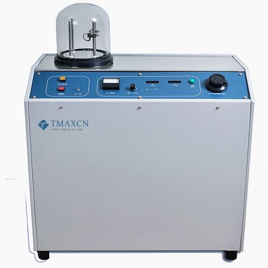
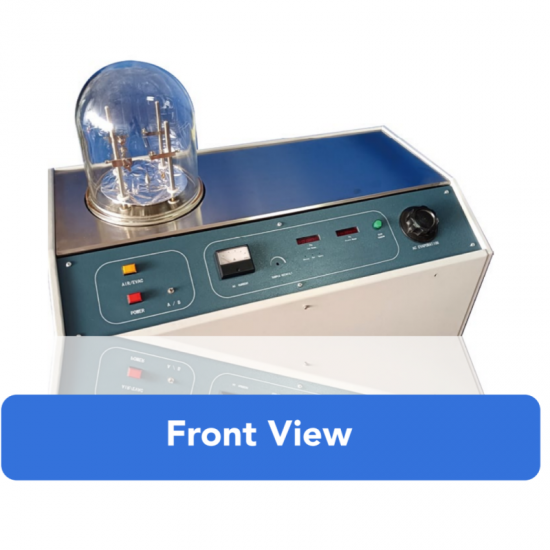
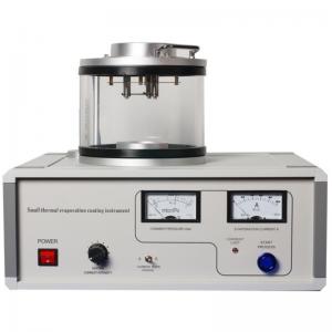
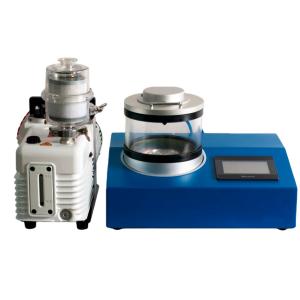
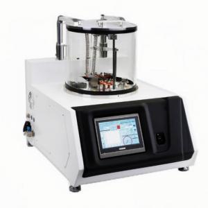
High Vacuum Thermal Evaporation Coater Evaporator System For High-Purity Metal Film Deposition
Model: Lith-BY-ZD06-High Vacuum Thermal Evaporation
Technical Specifications
|
Parameter
|
Specification
|
|
Evaporation Current
|
Max 100 A
|
|
Evaporation Voltage
|
Max 10 V
|
|
Heating Power
|
1,000 W
|
|
Chamber Size
|
Ø230 mm × 280 mm (H)
|
|
Working Vacuum
|
2×10⁻³ Pa
|
|
Ultimate Vacuum
|
2×10⁻⁴ Pa
|
|
Target Materials
|
Carbon, gold & other low-melting metals
|
|
Pumping System
|
Mechanical pump (primary) + Turbo molecular pump (secondary)
|
Key Features
✔ High Vacuum & Fast Deposition
· Advanced compound molecular pump ensures rapid gas evacuation for clean, efficient coating.
· Minimized oil backflow for contamination-free operation.
✔ Reliable & Efficient
· Resistive heating technology for stable evaporation of low-melting metals.
· Simple process with high deposition rates, ideal for lab-scale production.
✔ User-Friendly Design
· Compact chamber accommodates diverse sample sizes (up to Ø230 mm).
· Low maintenance costs for routine use in R&D and academia.
1. Non-Damaging Deposition
· Thermal Evaporation: Gentle heating avoids high-energy plasma, ideal for sensitive samples (e.g., polymers, biomaterials).
· Sputtering Risk: Energetic ions in sputtering may alter delicate surfaces.
2. Faster & Cleaner for Pure Metals
· Higher Deposition Rate: Rapid vaporization of metals (e.g., Au, C) reduces coating time.
· Sputtering Limitation: Slower for low-melting-point materials due to target cooling needs.
3. Minimal Sample Charging
· Uniform Conductive Layers: Smooth metal films (e.g., 5–10 nm Au) prevent SEM charging effectively.
· Sputtering Consideration: Sputtered films may exhibit grainier surfaces, affecting conductivity.
4. Lower Equipment Complexity
· No Gas/Plasma System: Simpler operation and maintenance vs. sputtering’s gas flow/power controls.
· Cost-Effective: Lower power consumption and consumable costs (e.g., replaceable tungsten boats).
Recommended Applications
· SEM Sample Preparation: Conductive coatings for non-conductive or beam-sensitive materials.
· Thin-Film Research: Rapid prototyping of pure metal films (Au, Ag, Al).
· Industrial R&D: Process optimization for specialty coatings.
Ideal For
· Microscopy Labs – Prevents charging in non-conductive samples.
· Material Scientists – Electrode fabrication & conductivity studies.
· Universities – Teaching tool for vacuum deposition principles.


 Online service
